If you are working in a decent workplace, you will receive lots of feedback on your code and what you do. Don't take it personal and learn from them. Sometimes there are multiple correct answers and yours can be one of them, but each workplace, project and senior colleague has their own concerns and priorities. Sometimes feedback seems to be on a trivial mundane detail, and sometimes it really will be. If you think it is valuable feedback, learn. If you disagree, discuss. Enjoy!
Polynomial Formal Verification: Verification-Centric Strategy
As formal verification becomes more common in the industry, design complexity continues to be a challenge. Article argues that this is a byproduct of design-centric approach (optimize area, power, speed) without considering verifiability. A verification-centric approach driven by polynomial formal verification analysis can produce verifiable designs.
Abstract: Recently, a lot of effort has been put into developing formal verification approaches by both academic and industrial research. In practice, these techniques often give satisfying results for some types of circuits, while they fail for others. A major challenge in this domain is that the verification techniques suffer from unpredictability in their performance. The only way to overcome this challenge is the calculation of bounds for the space and time complexities. If a verification method has polynomial space and time complexities, scalability can be guaranteed. In this tutorial paper, we review recent developments in formal verification techniques and give a comprehensive overview of Polynomial Formal Verification (PFV). In PFV, polynomial upper bounds for the run-time and memory needed during the entire verification task hold. Thus, correctness under resource constraints can be ensured. We discuss the importance and advantages of PFV in the design flow. Formal methods on the bit-level and the word-level, and their complexities when used to verify different types of circuits, like adders, multipliers, or ALUs are presented. The current status of this new research field and directions for future work are discussed.
5 Steps to Confront the Talent Shortage With IP-Centric Design
cross-posted from: https://discuss.tchncs.de/post/8824219
> One way to help alleviate the effects of the talent shortage is changing how semiconductors are designed so that organizations can achieve more with their existing workforce. This requires moving away from project-centric design and transitioning to an IP-centric design methodology. > > Over the past few years, teams have moved from building relatively self-contained, isolated designs to creating complex platforms across dispersed and integrated design centers. Larger design footprints, a more comprehensive array of products and quicker time to market are other contributing factors to walking away from a project-based design methodology.
5 Steps to Confront the Talent Shortage With IP-Centric Design
One way to help alleviate the effects of the talent shortage is changing how semiconductors are designed so that organizations can achieve more with their existing workforce. This requires moving away from project-centric design and transitioning to an IP-centric design methodology.
Over the past few years, teams have moved from building relatively self-contained, isolated designs to creating complex platforms across dispersed and integrated design centers. Larger design footprints, a more comprehensive array of products and quicker time to market are other contributing factors to walking away from a project-based design methodology.
It’s the manufacturing, stupid!
For battery-operated devices, the energy consumption for chip production far exceeds the lifetime energy consumption of the chips themselves. So, if we want to save energy, we’d better focus on the manufacturing process, argues Bram Nauta.
As you said before power on capacitor is discharged. Right after power on capacitor is still discharged, so voltage on capacitor is zero, so reset pin has Vcc. With time capacitor gets charges and voltage across capacitor increases and reset voltage becomes closer and closer to ground, until it is ground. But it is important to consider what happens at power down too. At power down capacitor is charged. If power source becomes high impedance at power down, then reset pin will probably go down to zero in time but may take a bit time depending on what source exactly does. But if power source is connected to zero at power down reset pin will observe minus vcc and slowly go up to 0. If reset pin is sensitive it may be a good idea to protect it with a diode.
If you knew about the birds and the bees, you would know that this wasn't random.
I don't know what it is. It just reminded me of ATMEL8051 and I wanted to share.
I used Atmel8051 in college. It fits nicely on a breadboard and teaches you how to use assembly and make wonders with 512 byte (yes byte) RAM if I remember the number correctly. I think half of that RAM was even reserved.
Immigration rules are getting stricter including higher min salary for skilled worker visa
The government has announced changes to some of its rules on legal migration to the UK.

To be fair 10^(0.000000000000000000001x) is also exponential growth. And if status quo is x=0 and removing entire management means x=10 this means even the max we can get is very little improvement. It can be "exponential" and still not so much.
"Exponentially" is not synonymous to "a lot". Exponent is a mathematical term and exponential growth requires at least two variables exponentially related to each other. For this to be possibly exponential growth a) progress should be quantifiable (removing management and treating workers well should be quantized somehow) b) performance should be quantifiable and measured at a bunch of progress points (if you have only two measurements it can as well be linear) c) performance should be or can be modeled as a an exponential function of progress in removing management and treating workers well.
Leakage resistance also contributes to dissipation factor and the simple formula omits this, that is why ESR calculated from dissipation factor is larger. As you said, if one is more interested in heat generated, dissipation factor is more important (leakage also dissipates power). If interested in the decoupling and filter performance of the capacitor, ESR is more important. And all these depend on temperature and capacitor bias voltage as well :)
I don't think this will work well and others already explained why, but thanks for using this community to pitch your idea. We should have more of these discussions here rather than CEO news and tech gossip.
I guess it can happen if you start moving the bottle forward after you start pouring the water.
We should stop calling these titles confusing and call them what they are, plain wrong. This is the title of the original article. People who cannot write grammatically correct titles are writing entire articles.
Grammatically speaking, doesn't it really say that Sunak warned others? I am confused.
Depending on the power consumption, you may consider not using thermal relief while connecting thermal vias for the chip (component 57) to ground layers. But this may make soldering harder so do it only if needed. Thermal vias are so close that they form 3 long dents in 3v3 plane. It is good practice to put vias a little far apart so that planes can go through between vias. This can be important since sometimes lowest impedance can be obtained when current is flowing between those vias. If you don't need to fit 15 vias there, you may consider reducing the number and separating them a bit. You can also check the design rules for minimum copper width and minimum via clearance for your manufacturer and enter them in your CAD tool.
I don't realistically expect such ban to happen. I started banning everyone who posts about Musk instead, my feed got a lot cleaner.
Why do people ask "Where does your name come from"?
I got this question multiple times while introducing myself. It sounds a bit odd and I don't think they are really interested in the origin of my name. Is this a politically correct way of asking my ethnic origin? I guess "Where are you from" wouldn't work for everyone since there are many born-and-raised British people with foreign names and ethnic origin.
Third siblings who were born right after cameras got affordable have the most pictures.
Universities, companies, and governments are forming broad partnerships to update skills and foster innovation in chips, security, AI, and related fields.

cross-posted from: https://discuss.tchncs.de/post/4827653
> So how can universities train students for a continuous and rapidly changing technology? This is especially difficult because it involves both software and hardware, and more domain-specific and increasingly heterogeneous architectures. And regardless of whether these devices are tethered to a battery or plugged into a socket, they need to be much more energy-efficient. Given the slowdown in Moore’s Law and the shrinking power, performance and area/cost benefits of scaling, that often requires a mix of computer science, electrical engineering, and in packages, an increasing amount of mechanical engineering. > > “Mechanical engineers, electrical engineers, those disciplinary trainings through those curriculums, they’re accredited and we have a very vigorous process that will continue. But these smaller, bite-sized chunks of curriculum will allow a student to broaden. So as a mechanical engineer, I may not necessarily have either capacity in my studies, or the depth of interest, to take an entire course on heterogeneous integration. But I might be very open to a smaller, bite-sized piece that’s looking at the thermal properties of packaging and new effects occurring because of things like heterogeneous integration. And that is going to be very important for us to be more nimble, to get these things done more quickly. > > “You could hire somebody who has a background in electrical engineering or computer engineering, where they understand the low-level hardware and how to build embedded systems and how to develop them, but they don’t usually have a background in securing them,” said Dan Walters, principal embedded security engineer and lead for microelectronics solutions at MITRE. “Or you could look at students with more of a focus in security and cybersecurity. Those typically are computer science degrees. And some universities have computer or cybersecurity degrees, but that’s really software-heavy. Those students don’t understand embedded systems and the unique things that come along with that. What we essentially did was hire from one of those two groups and say, ‘Okay, we’re going to do on-the-job training for the other 50% that you’re missing.'”
Chip Industry Talent Shortage Drives Academic Partnerships

So how can universities train students for a continuous and rapidly changing technology? This is especially difficult because it involves both software and hardware, and more domain-specific and increasingly heterogeneous architectures. And regardless of whether these devices are tethered to a battery or plugged into a socket, they need to be much more energy-efficient. Given the slowdown in Moore’s Law and the shrinking power, performance and area/cost benefits of scaling, that often requires a mix of computer science, electrical engineering, and in packages, an increasing amount of mechanical engineering.
“Mechanical engineers, electrical engineers, those disciplinary trainings through those curriculums, they’re accredited and we have a very vigorous process that will continue. But these smaller, bite-sized chunks of curriculum will allow a student to broaden. So as a mechanical engineer, I may not necessarily have either capacity in my studies, or the depth of interest, to take an entire course on heterogeneous integration. But I might be very open to a smaller, bite-sized piece that’s looking at the thermal properties of packaging and new effects occurring because of things like heterogeneous integration. And that is going to be very important for us to be more nimble, to get these things done more quickly.
“You could hire somebody who has a background in electrical engineering or computer engineering, where they understand the low-level hardware and how to build embedded systems and how to develop them, but they don’t usually have a background in securing them,” said Dan Walters, principal embedded security engineer and lead for microelectronics solutions at MITRE. “Or you could look at students with more of a focus in security and cybersecurity. Those typically are computer science degrees. And some universities have computer or cybersecurity degrees, but that’s really software-heavy. Those students don’t understand embedded systems and the unique things that come along with that. What we essentially did was hire from one of those two groups and say, ‘Okay, we’re going to do on-the-job training for the other 50% that you’re missing.'”
Oct. 9, 2023 — Edinburgh is poised to host a next-generation compute system amongst the fastest in the world, with the potential to advance breakthroughs in artificial intelligence, medicine, and […]

Exascale is the next frontier in computing power, where systems are built to carry out extremely complex functions with increased speed and precision. This in turn enables researchers to accelerate their work into some of the most pressing challenges we face, including the development of new drugs, and advances in nuclear fusion to produce potentially limitless clean low-carbon energy.
The exascale system hosted at the University of Edinburgh will be able to carry out these complicated workloads while also supporting critical research into AI safety and development, as the UK seeks to safely harness its potential to improve lives across the country.
I woke up today while trying to sync my breath to others. Does it happen to you?
I sleep with my wife and (when she graces us with her presence) our cat. Last night I caught myself syncing my breath to their breaths while sleeping, or half-sleeping considering I was aware of what was happening. Eventually their breathing went out of sync, and my breathing got confused, and after a very brief period of suffocation, I realized that I have no obligation to sync my breath, and took control of my breathing and started breathing normally. It felt strange to me but I googled it and it looks like syncing your breath happens to people. Does it happen to you as well?
PS: I realized while typing, I don't know if I should be hearing my 3kg cat's breathing. I should check on that.
Using LLMs to Facilitate Formal Verification of RTL
cross-posted from: https://discuss.tchncs.de/post/3979328
> Engineers in Princeton managed to train GPT4 and extend AutoSVA to generate SVA (systemverilog assertions) from buggy RTL and functionality description. SVA is widely used to verify digital design for ASIC and FPGAs. AutoSVA2, which extends open-source AutoSVA, improves the flow to generate SVA from English description. LLM was trained in multiple iterations to generate SVA with correct syntax, which is something GPT fails to do by itself. Authors argue that GPT's "creativity" allows it to write correct assertion even from a buggy RTL. Later authors used this tool to write RTL from scratch as well. RTL written by GPT was tested against the SVA generated by this tool, and SVA corrected by an engineer was fed back to LLM, which generated functionally correct FIFO queue in a few iterations. > > Abstract—Formal property verification (FPV) has existed for > decades and has been shown to be effective at finding intricate > RTL bugs. However, formal properties, such as those written as > SystemVerilog Assertions (SVA), are time-consuming and error- > prone to write, even for experienced users. Prior work has > attempted to lighten this burden by raising the abstraction level > so that SVA is generated from high-level specifications. However, > this does not eliminate the manual effort of reasoning and > writing about the detailed hardware behavior. Motivated by the > increased need for FPV in the era of heterogeneous hardware > and the advances in large language models (LLMs), we set out to > explore whether LLMs can capture RTL behavior and generate > correct SVA properties. First, we design an FPV-based evaluation > framework that measures the correctness and completeness of > SVA. Then, we evaluate GPT4 iteratively to craft the set of > syntax and semantic rules needed to prompt it toward creating > better SVA. We extend the open-source AutoSVA framework by > integrating our improved GPT4-based flow to generate safety > properties, in addition to facilitating their existing flow for liveness > properties. Lastly, our use cases evaluate (1) the FPV coverage of > GPT4-generated SVA on complex open-source RTL and (2) using > generated SVA to prompt GPT4 to create RTL from scratch. > Through these experiments, we find that GPT4 can generate > correct SVA even for flawed RTL—without mirroring design > errors. Particularly, it generated SVA that exposed a bug in the > RISC-V CVA6 core that eluded the prior work’s evaluation.
Using LLMs to Facilitate Formal Verification of RTL
Engineers in Princeton managed to train GPT4 and extend AutoSVA to generate SVA (systemverilog assertions) from buggy RTL and functionality description. SVA is widely used to verify digital design for ASIC and FPGAs. AutoSVA2, which extends open-source AutoSVA, improves the flow to generate SVA from English description. LLM was trained in multiple iterations to generate SVA with correct syntax, which is something GPT fails to do by itself. Authors argue that GPT's "creativity" allows it to write correct assertion even from a buggy RTL. Later authors used this tool to write RTL from scratch as well. RTL written by GPT was tested against the SVA generated by this tool, and SVA corrected by an engineer was fed back to LLM, which generated functionally correct FIFO queue in a few iterations.
Abstract—Formal property verification (FPV) has existed for decades and has been shown to be effective at finding intricate RTL bugs. However, formal properties, such as those written as SystemVerilog Assertions (SVA), are time-consuming and error- prone to write, even for experienced users. Prior work has attempted to lighten this burden by raising the abstraction level so that SVA is generated from high-level specifications. However, this does not eliminate the manual effort of reasoning and writing about the detailed hardware behavior. Motivated by the increased need for FPV in the era of heterogeneous hardware and the advances in large language models (LLMs), we set out to explore whether LLMs can capture RTL behavior and generate correct SVA properties. First, we design an FPV-based evaluation framework that measures the correctness and completeness of SVA. Then, we evaluate GPT4 iteratively to craft the set of syntax and semantic rules needed to prompt it toward creating better SVA. We extend the open-source AutoSVA framework by integrating our improved GPT4-based flow to generate safety properties, in addition to facilitating their existing flow for liveness properties. Lastly, our use cases evaluate (1) the FPV coverage of GPT4-generated SVA on complex open-source RTL and (2) using generated SVA to prompt GPT4 to create RTL from scratch. Through these experiments, we find that GPT4 can generate correct SVA even for flawed RTL—without mirroring design errors. Particularly, it generated SVA that exposed a bug in the RISC-V CVA6 core that eluded the prior work’s evaluation.
The semiconductor industry today is working to respond to a threefold mandate: increasing computing power, decreasing chip sizes and managing power in densely packed circuits.
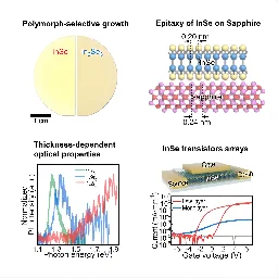
One of the biggest shortcomings of silicon is that it can only be made so thin because its material properties are fundamentally limited to three dimensions [3D]. For this reason, two-dimensional [2D] semiconductors—so thin as to have almost no height—have become an object of interest to scientists, engineers and microelectronics manufacturers.
Thinner chip components would provide greater control and precision over the flow of electricity in a device, while lowering the amount of energy required to power it. A 2D semiconductor would also contribute to keeping the surface area of a chip to a minimum, lying in a thin film atop a supporting silicon device.
But until recently, attempts to create such a material have been unsuccessful.
Now, researchers at the University of Pennsylvania School of Engineering and Applied Science have grown a high-performing 2D semiconductor to a full-size, industrial-scale wafer. In addition, the semiconductor material, indium selenide (InSe), can be deposited at temperatures low enough to integrate with a silicon chip.
"For the purposes of an advanced computing technology, the chemical structure of 2D InSe needs to be exactly 50:50 between the two elements. The resulting material needs a uniform chemical structure over a large area to work," says Song.
The team achieved this groundbreaking purity using a growth technique called "vertical metal-organic chemical vapor deposition" (MOCVD). Previous research had attempted to introduce the indium and selenium in equal quantities and at the same time. Song demonstrated, however, that this method was the source of undesirable chemical structures in the material, producing molecules with varying ratios of each element. MOCVD, by contrast, works by sending the indium in a continuous stream while introducing the selenium in pulses.
Why Is Computer Security Advice So Confusing?

The key takeaway here is that the people writing these guidelines try to give as much information as possible,” Reaves says. “That’s great, in theory. But the writers don’t prioritize the advice that’s most important. Or, more specifically, they don’t deprioritize the points that are significantly less important. And because there is so much security advice to include, the guidelines can be overwhelming – and the most important points get lost in the shuffle.
In other words, the guideline writers are compiling security information, rather than curating security information for their readers.
Drawing on what they learned from the interviews, the researchers developed two recommendations for improving future security guidelines.
First, guideline writers need a clear set of best practices on how to curate information so that security guidelines tell users both what they need to know and how to prioritize that information.
Second, writers – and the computer security community as a whole – need key messages that will make sense to audiences with varying levels of technical competence.
“Look, computer security is complicated,” Reaves says. “But medicine is even more complicated. Yet during the pandemic, public health experts were able to give the public fairly simple, concise guidelines on how to reduce our risk of contracting COVID. We need to be able to do the same thing for computer security.”
Advancing Cu-Cu Hybrid Bonding: Overcoming Challenges for the Future of Semiconductor Packaging | Microwave Journal
IDTechEx released the Advanced Semiconductor Packaging 2023-2033 and Materials and Processing for Advanced Semiconductor Packaging 2024-2034, reports. encapsulating their in-depth analysis and insights into the rapidly evolving landscape of 3D semiconductor packaging.
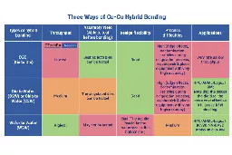
As solder bump pitches shrink, several issues arise. Reduced bump height and surface area for bonding make it increasingly difficult to establish reliable electrical connections, necessitating precise manufacturing processes to avoid errors. Critical co-planarity and surface roughness become paramount, as even minor irregularities can compromise successful bonding.
To overcome these issues, Cu-Cu hybrid bonding technology steps in as a game-changer. This innovative technique involves embedding metal contacts between dielectric materials and using heat treatment for solid-state diffusion of copper atoms, thereby eliminating the bridging problem associated with soldering.
The advantages of hybrid bonding over flip-chip soldering are obvious. Firstly, it enables ultra-fine pitch and small contact sizes, facilitating high I/O counts. This is critical in modern semiconductor packaging, where devices require a growing number of connections to meet performance demands. Secondly, unlike flip-chip soldering, which often relies on underfill materials, Cu-Cu hybrid bonding eliminates the need for underfill, reducing parasitic capacitance, resistance and inductance, as well as thermal resistance. Lastly, the reduced thickness of the bonded connections in Cu-Cu hybrid bonding, nearly eliminating the 10 to 30 micron thickness of solder balls in flip-chip technology, opens up new possibilities for more compact and efficient semiconductor packages.
Predicting the operational lifetime of solder joints in automotive applications.
cross-posted from: https://discuss.tchncs.de/post/3306215
> Although you are probably not aware of them, dozens of electronic control units (ECUs) — printed circuit boards (PCBs) in metal or plastic housings — exist in your car to control and monitor the operation and safety of your vehicle’s many control systems. These units must work for the lifetime of your car, during which time they are subjected to many heating and cooling cycles. The most obvious cycle occurs when you start your car after it has cooled at night. It heats up as the car runs and then cools again when you shut it off. That’s one “ambient” temperature cycle. > > Additional so called “active” thermal cycles can occur locally within specific electronic components on the PCB. For instance, a MOSFET transistor draws a lot of current and heats up the PCB near its location, causing additional thermal cycling. These complex temperature distributions can cause local thermomechanical strain because differences in temperature across the PCB result in differential expansion of the board. Because the board is constrained by its housing, this can lead to bending of the board, putting additional strain on the solder joints that connect the components to the board. > > The widely used power law based approach — simulation of only few cycles and prognosis of solder joints lifetime — has many shortcomings, where no absolute lifetime prediction or the damage driven load relocation and its nonlinear evolution are captured. Youssef Maniar and Marta Kuczynska, engineers at Robert Bosch GmbH in Germany, have developed an accurate nonlinear damage model able to predict absolute lifetime of solder connections. The problem they faced, absolute lifetime prediction, involves simulation of all cycles imposed to the components, and the computational effort is therefore extensive. Then, about two years ago, they read an academic paper that described a way to “jump” over some cycles to accelerate simulation. > > The mathematics behind the ability to jump over a large number of simulated thermomechanical cycles to dramatically accelerate the simulation time without sacrificing accuracy is involved, but the software essentially looks at the slope or “gradient” of certain solution variables (e.g., stress) versus time plot on the fly to determine when it can skip over the next n number of cycles. The maximum value of n must be defined by the simulation engineer before the run. The simulation engineer also inputs other parameters beforehand to impose limits on the software to optimize the run.
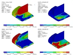
Jumping Over Thermal Cycles Accelerates Thermomechanical Fatigue Simulations

Although you are probably not aware of them, dozens of electronic control units (ECUs) — printed circuit boards (PCBs) in metal or plastic housings — exist in your car to control and monitor the operation and safety of your vehicle’s many control systems. These units must work for the lifetime of your car, during which time they are subjected to many heating and cooling cycles. The most obvious cycle occurs when you start your car after it has cooled at night. It heats up as the car runs and then cools again when you shut it off. That’s one “ambient” temperature cycle.
Additional so called “active” thermal cycles can occur locally within specific electronic components on the PCB. For instance, a MOSFET transistor draws a lot of current and heats up the PCB near its location, causing additional thermal cycling. These complex temperature distributions can cause local thermomechanical strain because differences in temperature across the PCB result in differential expansion of the board. Because the board is constrained by its housing, this can lead to bending of the board, putting additional strain on the solder joints that connect the components to the board.
The widely used power law based approach — simulation of only few cycles and prognosis of solder joints lifetime — has many shortcomings, where no absolute lifetime prediction or the damage driven load relocation and its nonlinear evolution are captured. Youssef Maniar and Marta Kuczynska, engineers at Robert Bosch GmbH in Germany, have developed an accurate nonlinear damage model able to predict absolute lifetime of solder connections. The problem they faced, absolute lifetime prediction, involves simulation of all cycles imposed to the components, and the computational effort is therefore extensive. Then, about two years ago, they read an academic paper that described a way to “jump” over some cycles to accelerate simulation.
The mathematics behind the ability to jump over a large number of simulated thermomechanical cycles to dramatically accelerate the simulation time without sacrificing accuracy is involved, but the software essentially looks at the slope or “gradient” of certain solution variables (e.g., stress) versus time plot on the fly to determine when it can skip over the next n number of cycles. The maximum value of n must be defined by the simulation engineer before the run. The simulation engineer also inputs other parameters beforehand to impose limits on the software to optimize the run.
What is your comfort activity (like comfort food)?
Mine is playing AOE2 in easiest (or standard if I want a bit of challenge) mode against 3 bots. I just build my economy, wall up (and laugh at the enemy soldiers attacking my walls in vain), reach imperial age and attack once my army reaches the population limit. I also send 104 in the chat so they don't surrender and I can enjoy razing their all buildings one by one. If any of them builds a castle, even more fun. A build a trebuchet and watch it raze the castle from a safe distance. If there is sea, after I am done with the land, I build 3 docks, do research and build a navy and hunt down ships around the unxplored sea. It is fun, satisfying and relaxing.
What is yours?
Test Strategies In The Era Of Heterogeneous Integration

cross-posted from: https://discuss.tchncs.de/post/3157319
> Compared with traditional monolithic devices, the design and manufacturing process for chiplets is significantly different. The scrap costs associated with manufacturing traditional monolithic semiconductor devices is basically linear, including single chip cost, packaging, and assembly costs. > > Manufacturing processes for 2.5D/3D designs differ significantly in terms of the accumulation of scrap costs. Specifically, these costs increase geometrically from fabrication to assembly driven by scrap costs for multiple dies, multi-chip partial assemblies, and/or full 2.5D/3D packages. > > Shifting tests, either left or right, in the test process is a strategy to achieve these goals and minimize the overall manufacturing cost of 2.5D/3D components. Shift left is the ability to increase test coverage earlier in the manufacturing process (e.g., during wafer inspection and partial packaging) to maximize KGD, while reducing future packaging costs. Additional tests can also be added to the process to identify new failure types or failure modes. > > However, the benefits of shift left need to be weighed. For example, increasing test intensity early in the manufacturing process can positively impact known good devices but it can also lead to an increase in test costs that is not sufficiently offset by the optimizations, even after accounting for the resulting reduction in scrap costs. > > Shift right means increasing test coverage later in the manufacturing process, expanding the ability to detect defects, and maintaining quality levels with the goal of reducing costs with higher parallelism testing. > > Typically, a test item with a higher yield on wafer or mission pattern tests, or a high yield test that requires a longer scan test time is an ideal candidate for shifting right. These tests can be moved to final or system level test, or flexibly managed in between. > > The goal of shifting tests to the left or right is to achieve the optimal combination of quality and yield throughout the entire manufacturing process, ultimately optimizing the overall cost of quality. >
When dealing with complex test processes, optimizing the total cost of quality is critical.
Compared with traditional monolithic devices, the design and manufacturing process for chiplets is significantly different. The scrap costs associated with manufacturing traditional monolithic semiconductor devices is basically linear, including single chip cost, packaging, and assembly costs.
Manufacturing processes for 2.5D/3D designs differ significantly in terms of the accumulation of scrap costs. Specifically, these costs increase geometrically from fabrication to assembly driven by scrap costs for multiple dies, multi-chip partial assemblies, and/or full 2.5D/3D packages.
Shifting tests, either left or right, in the test process is a strategy to achieve these goals and minimize the overall manufacturing cost of 2.5D/3D components. Shift left is the ability to increase test coverage earlier in the manufacturing process (e.g., during wafer inspection and partial packaging) to maximize KGD, while reducing future packaging costs. Additional tests can also be added to the process to identify new failure types or failure modes.
However, the benefits of shift left need to be weighed. For example, increasing test intensity early in the manufacturing process can positively impact known good devices but it can also lead to an increase in test costs that is not sufficiently offset by the optimizations, even after accounting for the resulting reduction in scrap costs.
Shift right means increasing test coverage later in the manufacturing process, expanding the ability to detect defects, and maintaining quality levels with the goal of reducing costs with higher parallelism testing.
Typically, a test item with a higher yield on wafer or mission pattern tests, or a high yield test that requires a longer scan test time is an ideal candidate for shifting right. These tests can be moved to final or system level test, or flexibly managed in between.
The goal of shifting tests to the left or right is to achieve the optimal combination of quality and yield throughout the entire manufacturing process, ultimately optimizing the overall cost of quality.